Which of the following options describes correctly the equilibrium band diagram at T = 300 K of a silicon pnn+ p++ configuration shown in the figure?
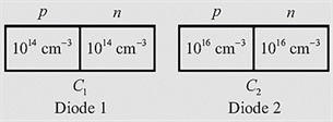
As shown, two Silicon (Si) abrupt p-n junction diodes are fabricated with uniform donor doping concentrations of = 1014 cm–3 and = 1016 cm–3 in the n-regions of the diodes, and uniform acceptor doping concentrations of = 1014 cm–3 and = 1016 cm–3 in the p-regions of the diodes, respectively. Assuming that the reverse bias voltage is >> built-in potential of the diodes, the ratio of their reverse bias capacitances for the same applied reverse bias is ______.
Red (R), Green (G) and Blue (B) Light Emitting Diodes (LEDs) were fabricated using p-n junctions of three different inorganic semiconductors having different band-gaps. The built-in voltages of red, green and blue diodes are VR, VG and VB, respectively. Assumed donor and acceptor doping to be the same (NA and ND, respectively) in the p and n sides of all the three diodes.
Which one of the following relationships about the built-in voltages is TRUE?
A region of negative differential resistance is observed in the current voltage characteristics of a silicon p-n junction if
In a p-n junction diode at equilibrium, which one of the following statements is NOT TRUE?
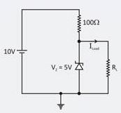
In the circuit shown below, the knee current of ideal zener diode is 10 mA. To maintain 5 volts across the load RL, the minimum value of RL in ’s and the minimum power rating of the zener diode in mW respectively are
The ripple factor in a full wave rectifier without filter is
Consider the following rectifier circuits
1. Have – wave rectifier without filter.
2. Full – wave rectifier without filter.
3. Full – wave rectifier with series inductance filter.
4. Full – wave rectifier with capacitance filter.
The sequence of these rectifier circuits in decreasing order of their ripple factor is.
The use of a rectifier circuit in a capacitor filter gives satisfactory performance only when the load
The PIV rating of the diodes used in power supply circuits are chosen by which one of the following criteria?
Silicon diodes are less suitable for low voltage rectifier operation because.
The ripple frequency in a full wave rectifier is…………..that of the supply frequency.
