github

Made bySaurav Hathi

ECE - Practice Test - 18

Q1:

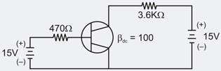
From the following figure, find the collector current?

Tags:
PlaceMe2_BE&EDC3
NEAT_BE&EDC3
Section:
Basic Electronics
Options:
Q2:

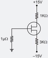
The current source-bias circuit is given below. The voltage between the drain and ground will be?

Tags:
PlaceMe2_BE&EDC3
NEAT_BE&EDC3
Section:
Basic Electronics
Options:
Q3:

MOSFET is in triode region for

Tags:
PlaceMe2_BE&EDC3
NEAT_BE&EDC3
Section:
Basic Electronics
Options:
Q4:

In E - MOSFET, channel does not form initially due to

Tags:
PlaceMe2_BE&EDC3
NEAT_BE&EDC3
Section:
Basic Electronics
Options:
Q5:

In a common base configuration, current gain is 0.97. If the emitter current is 1mA, the value of base current is

Tags:
PlaceMe2_BE&EDC3
NEAT_BE&EDC3
Section:
Basic Electronics
Options:
Q6:

The larger input resistance of the MOSFET is due to

Tags:
PlaceMe2_BE&EDC3
NEAT_BE&EDC3
Section:
Basic Electronics
Options:
Q7:

N channel FETs are superior to P-channel FETs because

Tags:
PlaceMe2_BE&EDC3
NEAT_BE&EDC3
Section:
Basic Electronics
Options:
Q8:

At pinch-off voltage, applied on the gate in a JFET

Tags:
PlaceMe2_BE&EDC3
NEAT_BE&EDC3
Section:
Basic Electronics
Options:
Q9:

If a transistor is operating with both of its junctions forward biased, but with the collector base forward bias greater than the emitter-base forward bias, then it is operating in the

Tags:
NEAT_ECE_Exit_Baseline
PlaceMe2_BE&EDC3
NEAT_BE&EDC3
Section:
Basic Electronics
Options:
Q10:

The inversion charge accumulated in MOSFET channel wide near,

Tags:
PlaceMe2_BE&EDC3
NEAT_BE&EDC3
Section:
Basic Electronics
Options:
Q11:

When a step- input is given to an op-amp integrator, the output will be

Tags:
PlaceMe2_BE&EDC3
NEAT_BE&EDC3
Section:
Basic Electronics
Options:
Q12:

The minority carriers in NPN and PNP transistors are

Tags:
PlaceMe2_BE&EDC3
NEAT_BE&EDC3
Section:
Basic Electronics
Options:
Q13:

In NPN Transistor, the doping concentration of base is

Tags:
PlaceMe2_BE&EDC3
NEAT_BE&EDC3
Section:
Basic Electronics
Options:
Q14:

The relation between the α & β of a transistor is given by

Tags:
PlaceMe2_BE&EDC3
NEAT_BE&EDC3
Baseline3_ECE_2Yr
Section:
Basic Electronics
Options:
Q15:

The lowest output impedance is obtained in case of BJT amplifiers for

Tags:
PlaceMe2_BE&EDC3
NEAT_BE&EDC3
Section:
Basic Electronics
Options: