In IC fabrication, harmful impurities or defects are removed from the region in a wafer. This process is termed as
The sequence of steps involved in fabrication of poly silicon gate MOSFET?
Step1: Entire water surface of a Si3Ni is coated & it is etched away with the help of mock to include source, gate & drain.
Step2: The contact areas are defined using photolithographic process.
Step3: Etching of Si3N4 & thin oxide growth selective.
Step4: Depletion of poly silicon gate.
Step5: Thick oxide growth called field oxide & P implantation.
Step6: Metallization & interconnection between substrate & source.
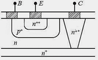
The correct circuit representation of the structure shown in the figure is
Which of the following is most difficult to fabricate in an IC?
MOSFET wafers are oriented in
Monolithic Integrated circuits exhibits
Dual-in-Line pack is considered to be suitable for mounting because,
In MOSFET fabrication, the channel length is defined during the process of
What effect does a metal semiconductor work function difference have on a C(V) characteristic for an MOS capacitor?
Using transistors as:
1. Class-A power amplifier has a minimum efficiency of 50%
2. Class-B push-pull power amplifier gives rise to crossover distortion.
3. Class AB push-pull power amplifier has higher efficiency than Class B push-pull amplifiers
4. Class-C power amplifier is generally used with tuned load for RF amplifications.
Which of these statements are correct?
If the 100mv is fed from the output back to the input and output of amplifier is assumed to be 10V, then feedback fraction will be
Consider the following:
1.Distortion
2.Gain
3.Bias stabilization
4.Sensitivity
5.Frequency response
Which of these properties of the power amplifier one should concentrate upon while designing a good power amplifier circuit?
The lowest output impedance is obtained in case of BJT amplifiers for
Which one of the following power amplifiers has the maximum efficiency?
Negative feedback in an amplifier
