An n+-n Silicon device is fabricated with uniform and non-degenerate donor doping concentrations of = 1 × 1018 cm–3 and = 1 × 1015 cm–3 corresponding to the n+ and n regions respectively. At the operational temperature T, assume complete impurity ionization, kT/q = 25 mV, and intrinsic carrier concentration to be ni = 1 × 1010 cm–3. What is the magnitude of the built-in potential of this device?
Group-I lists four different semiconductor devices. Match each device in Group-I with its characteristic property in Group-II
|
Group-I |
Group-II |
||
|
P |
BJT |
1 |
Population Incision |
|
Q |
MOS Capacitor |
2 |
Pinch-off voltage |
|
R |
LASER diode |
3 |
Early Effect |
|
S |
JFET |
4 |
Flat-band voltage |
Contact potential of diode with temperature
When PN junction diode is forward bias then its depletion layer width.
Contact potential for ‘si’ diode
Depletion layer consists of :-
Before power amplifiers, the amplification of audio signal is done by
In switching diode fabrication dopant is introduced into silicon which introduces additional trap level in the material there by reducing the mean life of carriers. This dopant is
Find the forward current of a Ge diode operating at 300k with forward voltage of 100mv across it. Assume saturation current of 20𝜇a
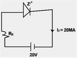
Find the value limiting resistance (Rs) required for the LED circuit is given below
An ideal op- amp is a
The ideal op-amp has the following characteristics.
When a step- input is given to an op-amp integrator, the output will be
For an op-amp having differential gain Av and common-made gain Ac, the CMRR is given by
In depletion MOSFET, the channel is
An n - channel JFET has IDSS = 2mA and Vp = – 4V. Its thermo conductance gm=in (in mA/V) for an applied GATE to voltage VGS of – 2V is
Consider an ideal n-channel MOSFET with parameters L = 1.25 µn, µn = 650 cm2/V-s, Cox = 6.9 × 10⁻⁸ F/cm2, and VT = 0.65 V. If VGS = 5V and ID(sat) = 4 mA then channel width will be?
The source of a silicon (ni = 1010 per cm3) n - channel MOS transistor has an area of 1 sq µm and a depth of 1 µm. If the dopant density in the source is 1019 / cm3, the number of holes in the source region with the above volume is approx.
The emitter is always forward biased with respect to base?
The lowest output impedance is obtained in case of BJT amplifiers for
