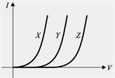
The I-V characteristics of three types of diodes at the room temperature, made of semiconductors X, Y and Z, are shown in the figure. Assume that the diodes are uniformly doped and identical in all respects except their materials. If EgX, EgY and EgZ are the band gaps of X, Y and Z, respectively, then
Arrange in order first to last
1. Metal contacts
2. Source and drain doping
3. Field oxidation
4. Gate oxidation
Depletion layer help which type of carriers in crossing the junction ?
A zener diode when used in voltage stabilization circuits is biased in.
The reverse current of a silicon diode is
When a positive die voltage is applied to the n-side relative to P-side a diode is said to be give
When the optical power incident on a photodiode is 10W and the responsively is 0.8 A/W, the photocurrent generated (in A) is
Consider an n-type silicon photoconductor with a length L = 100m, cross sectional area A = 10–7 cm2, and minority carrier lifetime S. The gain of a silicon photoconductor will be (Assume V = 10v)
Which diode would be most suitable for a tuning circuit?
For an op-amp having differential gain Av and common-made gain Ac, the CMRR is given by
In a differential Amplifier, CMRR can be improved by using an increased.
A change in the value of the emitter resistance (Re) in a Differential Amplifier
One input terminal of high gain comparator circuit is connected to ground and a sinusoidal voltage is applied to its other input. The output of comparator will be.
In JFET
|
List I |
List II |
|
A) The pinch off voltage decreases. |
1) The channel doping is reduced. |
|
B) The trans conductance increases. |
2) The channel length is increases. |
|
C) The transit time of the carrier in the channel is reduced. |
3) The conductivity of the channel in increased. |
|
|
4) The channel length is reduced. |
|
|
5) The GATE area is reduced. |
Which has minimum noise disturbance
For MOSFET to work as a switch it must operate in
Oxide parasitic capacitance in MOSFET is formed between
In a Zener diode
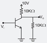
The transistor in the circuit below is biased at a dc collector current of 0.5mA. What is the voltage gain?
For a BJT, Vt is 5V, RC = 1000 & bias current IC is 12mA. The value of voltage gain is
