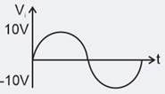
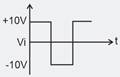
The correct form wave from for O/P for the below network is.
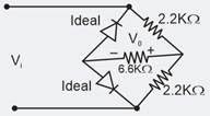
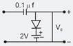
Mention resistance value across which V0 is determined
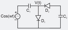
The diodes and capacitors in the circuit shown are ideal. The voltage V(t) across the diode D1 is.
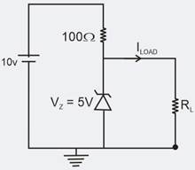
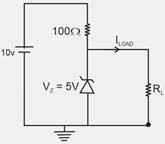
In the circuit shown below. The knee current of the ideal zener diode is 10mA. To maintain 5V across RL, the minimum value of RL in and the maximum power rating of the zener diode in mW, respectively are
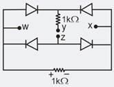
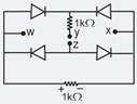
A voltage 1000 Sin wt volts is applied across yz. Assuming ideal diodes, the voltage measured across WX in volts is,
In the circuit shown below, assume that the voltage drop across a forward biased diode is 0.7V. The thermal voltage Vt=KT/2=25mV. The small signal input Vi=Vpcos(wt) where Vp = 100mV
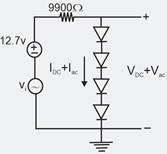
The ac output voltage Vac is
The wave shape of V0 in fig is
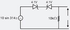
A voltage volts is applied across YZ. Assuming ideal diodes, the voltage measured across WX in volts is,
Select the correct output wave-shape for a given input in the clamping network given below:
In the circuit shown below. The knee current of the ideal zener diode is 10mA. To maintain 5V across RL, the minimum value of RL in and the maximum power rating of the zener diode in mW, respectively are
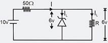
The 6V zener diode shown below has zero zener resistance and a knee current of 5mA. The minimum value of R. so that the voltage across if does not fall below 6V is.
Consider the following rectifier circuits
1. Have – wave rectifier without filter.
2. Full – wave rectifier without filter.
3. Full – wave rectifier with series inductance filter.
4. Full – wave rectifier with capacitance filter.
The sequence of these rectifier circuits in decreasing order of their ripple factor is.
Silicon diodes are less suitable for low voltage rectifier operation because.
Consider the following statements
A clamper circuit:
1. Adds or subtracts a dc voltage to or from a waveform
2. Does not change the shape of the waveform
3. Amplifies the waveform
The PIV rating of the diodes used in power supply circuits are chosen by which one of the following criteria?
The maximum efficiency of half-wave rectifier considering ideal diode?
