Assertion (A): Op-amp with FET input stages have less gain than those BJT.
Reason(R): BJT has higher trans conductance than FET.
Consider the following devices.
1. BJT in CB mode
2. BJT in CE mode
3.JFET
4.MOSFET
The correct sequence of these devices in increasing order of their input impedance is:
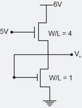
In the circuit show below, for the MOS transistor and the threshold Voltage The Voltage VX at the source of the upper transistor is
The Gain of a MOSFET Amplifier drops at very low frequencies due to -
The current gain of a bipolar transistor drops at high frequency because of
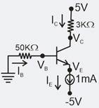
A Si transistor with is used as shown in the below figure. Then the minimum value of for which transistor remains in the saturation region
![]()
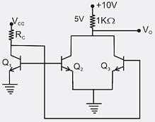
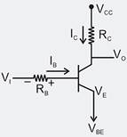
Determine the DC current ‘Ic’ for the circuit shown below. Assuming
The circuit using a BJT with and is shown in the figure. The base current and collector voltage VC are respectively
The transistor switch as shown in figure has =120,=0.2V. =1.2k and =5V
The output voltage when transistor switch is closed and the minimum base current needed to close the switch, are respectively.
Assertion (A): A fixed bias BJT circuit exhibits better performance as compared to a self bias BJT circuit.
Reason (R): A fixed bias BJT circuit uses less components as compared to a self bias BJT circuit.
A BJT is said to be operating in the saturation region if:
Why n-p-n transistors are preferred over p-n-p transistor?
Biasing is used in transistor amplifiers to
1. Stabilize the operating point against temperature variation.
2. Place the operating point in the linear region of the characteristics.
3. Make ,and ICO of the transistor independent of temperature variation.
4. Reduce distortion and increases dynamic range.
The current gain of a bipolar transistor drops at high frequency because of:
The phenomenon known as ‘early effect’ in a bipolar transistor refers to a reduction of the effective base which is caused by
