Match List-I (type of amplifier) with List-II (property) and select the correct relation between the Lists?
|
List-I |
List-II |
|
A. Single ended class- A |
1. Meduim efficiency with minimum distortion. |
|
B .Class - AB push-pull |
2. High efficiency with cross over distortion. |
|
C. Class - B push-pull |
3. Harmonic generator with highest possible conversion efficiency |
|
D. Class - C. |
4. Poor conversion efficiency with minimum distortion. |
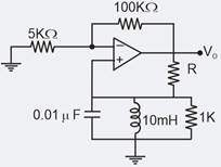
Value of R in the Oscillator shown in the given figure is so chosen that it just oscillates at an angular frequencies of . The value of ‘’ and the required Value of R will respectively be
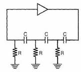
The Oscillator Circuit shown in the figure has an ideal inverting amplifier it frequency of oscillation (in HZ) is
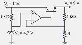
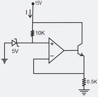
In the voltage regulator circuit shown in the figure, the op-amp is ideal. The BJT has VBE = 0.7 V and = 100, and the zener voltage is 4.7 V. For a regulated output of 9V, the value of R(in ) is………. .
Consider the Schmidt trigger circuit shown below
A triangular wave which goes from –12V to 12V is applied to the inverting input of the OPAMP. Assume that the output of the OPAMP swings from+15V to –15V. The voltage at the non-inverting input switches between
What is the impact on input and output impedances in current amplifier feedback topology?
Trans conductance amplifier is also named as?
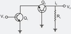
In the cascade amplifier shown in the given figure, if the common – emitter stage (Q1) has a trans conductance gm1, and the common base stage (Q2) has a trans conductance gm2, then the overall trans conductance g( = i0/vi) of the cascade amplifier is
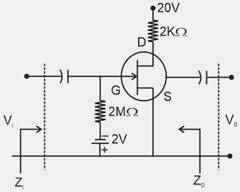
A JFET (with tuned load in the drain Circuit) is operated as a tuned Amplifier. Given for the FET and for the drain circuit is parallel with.
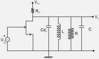
The magnitude of Voltage gain of the amplifier at resonance is ………… .
An Amplifier has two identical Cascaded Stages. Each stages has a bandwidth of 20 KHZ. The overall bandwidth shall approximately be equal to
A small Signal Voltage amplifier in common emitter configuration was working satisfactorily. Suddenly its emitter- bypass Capacitor (CE) got disconnected its
1. Voltage gain will decrease
2. Voltage gain will increase.
3. Bandwidth will decrease.
4. Bandwidth will increase.
Which of these statements are correct?
In the circuit shown find the value of I (mA)
Which one of the following statement is correct.
The rise time of an amplifier is
In the circuit shown below, capacitors C1 and C2 are very large and are shorts at the input frequency. vi is a small signal input. The gain magnitude |v0/vi| at 10 Mrad/s is
Given
and of the circuit are respectively
A dc power supply has a no-load voltage of 30V and a full-load voltage of 25V at a full load current of 1A. Its output resistance and load regulation, respectively are
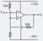
One input terminal of high gain comparator circuit is connected to ground and a sinusoidal voltage is applied to the other input. The output of comparator will be.
A BJT is to be used in a high freq. circuit in common emitter amplifier. For a higher upper cut-off frequency ( and have their usual meanings)
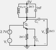
In the following Si BJT circuit if
The value of to maintain the operating point
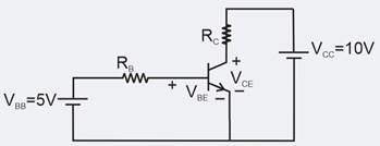
Rc=0.5
|
List-I |
List-II |
|
A. The current gain of a BJT will be increased . |
1. The collector doping concentration is increased. |
|
B. The current gain of a BJT will be reduced. |
2. The base width is reduced. |
|
C. The break-down voltage of a BJT will be reduced. |
3. The emitter doping concentration to base doping concentration ratio is reduced. |
